- 您现在的位置:买卖IC网 > Sheet目录250 > SFCF2048H1BO2TO-I-M0-523-SMA (Swissbit NA Inc)FLASH SLC UDMA/MDMA/PIO 2G
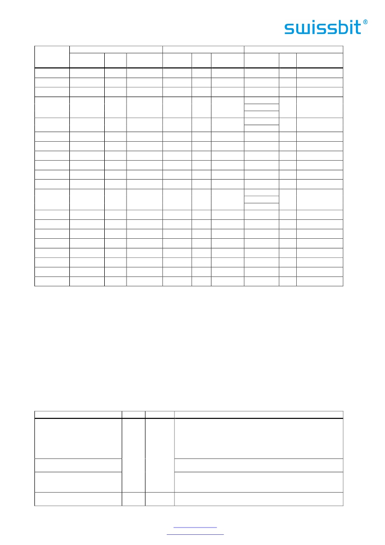
Pin Num
PC Card Memory Mode
PC Card I/O Mode
True IDE Mode (4)
Signal
Name
Pin
Type
In, Out
Type
Signal
Name
Pin
Type
In, Out
Type
Signal
Name
Pin
Type
In, Out
Type
31
32
33
D15 (1)
-CE2 (1)
-VS1
I/O
I
O
I1Z,OZ3
I3U
Ground
D15 (1)
-CE2 (1)
-VS1
I/O
I
O
I1Z,OZ3
I3U
Ground
D15 (1)
-CS1 (1)
-VS1
I/O
I
O
I1Z,OZ3
I3Z
Ground
-IORD (7)
34
-IORD
I
I3U
-IORD
I
I3U
HSTROBE (8)
I
I3Z
-HDMARDY (9)
35
36
37
-IOWR
-WE
READY
I
I
O
I3U
I3U
OT1
-IOWR
-WE
-IREQ
I
I
O
I3U
I3U
OT1
-IOWR (7)
STOP (8)(9)
-WE (3)
INTRQ
I
I
O
I3Z
I3U
OZ1
38
Vcc
Power
Vcc
Power
Vcc
Power
39
40
41
-CSEL (5)
-VS2
RESET
I
O
I
I2Z
OPEN
I2Z
-CSEL (5)
-VS2
RESET
I
O
I
I2Z
OPEN
I2Z
-CSEL
-VS2
-RESET
I
O
I
I2U
OPEN
I2Z
IORDY (7)
42
-WAIT
O
OT1
-WAIT
O
OT1
-DDMARDY (8)
O
ON1
DSTROBE (9)
43
-INPACK
O
OT1
-INPACK
O
OT1
DMARQ
O
OZ1
44
-REG
I
I3U
-REG
I
I3U
-DMACK
(6)
I
I3U
45
46
BVD2
BVD1
I/O
I/O
I1U,OT1
I1U,OT1
-SPKR
-STSCHG
I/O
I/O
I1U,OT1
I1U,OT1
-DASP
-PDIAG
I/O
I/O
I1U,ON1
I1U,ON1
47
D08
(1)
I/O
I1Z,OZ3
D08
(1)
I/O
I1Z,OZ3
D08
(1)
I/O
I1Z,OZ3
48
D09
(1)
I/O
I1Z,OZ3
D09
(1)
I/O
I1Z,OZ3
D09
(1)
I/O
I1Z,OZ3
49
D10
(1)
I/O
I1Z,OZ3
D10
(1)
I/O
I1Z,OZ3
D10
(1)
I/O
I1Z,OZ3
50
GND
Ground
GND
Ground
GND
Ground
1.
2.
3.
4.
5.
6.
7.
8.
9.
These signals are required only for 16 bit accesses and not required when installed in 8 bit systems.
Devices should allow for 3-state signals not to consume current.
The signal should be grounded by the host.
The signal should be tied to VCC by the host.
The mode is required for CompactFlash Storage Cards.
The – CSEL signal is ignored by the card in PC Card modes. However, because it is not pulled up on the card
in these modes, it should not be left floating by the host in PC Card modes. In these modes, the pin
should be connected by the host to PC Card A25 or grounded by the host.
If DMA operations are not used, the signal must be held high or tied to VCC by the host, also for read
registers.
Signal usage in True IDE Mode except when Ultra DMA mode protocol is active.
Signal usage in True IDE Mode when Ultra DMA mode protocol DMA Write is active.
Signal usage in True IDE Mode when Ultra DMA mode protocol DMA Read is active. The signal should be
grounded by the host.
Table 12: Signal Description
Signal Name
Dir.
Pin
Description
These address lines along with the – REG signal are used to
select the following: The I/O port address registers within the
A10 to A0
(PC Card Memory Mode)
I
CompactFlash Storage Card, the memory mapped port address
registers within the CompactFlash Storage Card, a byte in the
8,10,11,12, card ’ s information structure and its configuration control and
14,15,16,17, status registers.
A10 to A0
(PC Card I/O Mode)
A2 to A0
(True IDE Mode)
18,19,20
This signal is the same as the PC Card Memory Mode signal.
In True IDE Mode, only A[2:0] are used to select the one of eight
registers in the Task File, the remaining address lines should be
grounded by the host.
BVD1
(PC Card Memory Mode)
I/O
46
This signal is asserted high, as BVD1 is not supported.
Swissbit AG
Industriestrasse 4
Swissbit reserves the right to change products or specifications without notice.
Revision: 1.20
CH-9552 Bronschhofen
Switzerland
www.swissbit.com
industrial@swissbit.com
C-320_data_sheet_CF-HxBO_Rev120.doc
Page 12 of 101
发布紧急采购,3分钟左右您将得到回复。
相关PDF资料
SFCF4096H4BK2SA-I-QT-553-SMA
FLASH SLC UDMA/MDMA/PIO 4G
SFCF64GBH2BU4TO-I-NU-517-STD
FLASH SLC UDMA/MDMA/PIO 64GB
SFN08B4702CBQLF7
RES ARRAY 47K OHM 7 RES 8-DFN
SFP1050-12BG
FRONT END AC/DC 1050W 12V
SFP450-12BG
PWR SUP 450W 12V 36.6A W/STANDBY
SFSD1024N1BN1TO-I-DF-151-STD
FLASH MICRO SD CARD IND S-200 1G
SFSD2048L1BN2TO-I-DF-151-STD
FLASH SECURE DGTL CARD SD 2G
SFSD4096L1BN2TO-I-Q2-141-STD
FLASH SECURE DGTL CARD SDHC 4G
相关代理商/技术参数
SFCF2048H1BO2TO-I-M0-533-ZP1
制造商:SWISSBIT NA INC 功能描述:FLASH
SFCF2048H1BO2TO-I-M0-543-SMA
制造商:SWISSBIT NA INC 功能描述:FLASH
SFCF2048H2BU2TO-C-MS-527-STD
制造商:SWISSBIT NA INC 功能描述:FLASH
SFCF2048H2BU2TO-I-MS-517-STD
功能描述:FLASH SLC UDMA/MDMA/PIO 2GB RoHS:是 类别:存储卡,模块 >> 存储器,PC 卡 系列:C-440 标准包装:30 系列:- 存储容量:8GB 存储器类型:存储卡 - Extreme III SD?
SFCF2048H2BU2TO-I-MS-527-STD
制造商:SWISSBIT NA INC 功能描述:FLASH
SFCF2048H4BK1SA-C-QT-553-SMA
制造商:SWISSBIT NA INC 功能描述:FLASH
SFCF2048H4BK1SA-I-QT-553-SMA
功能描述:FLASH SLC UDMA/MDMA/PIO 2G RoHS:是 类别:存储卡,模块 >> 存储器,PC 卡 系列:C-300 标准包装:30 系列:- 存储容量:8GB 存储器类型:存储卡 - Extreme III SD?
SFCF2048H4BK2SA-C-DS-553-SMA
制造商:SWISSBIT NA INC 功能描述:FLASH SLC UDMA/MDMA/PIO 2G